

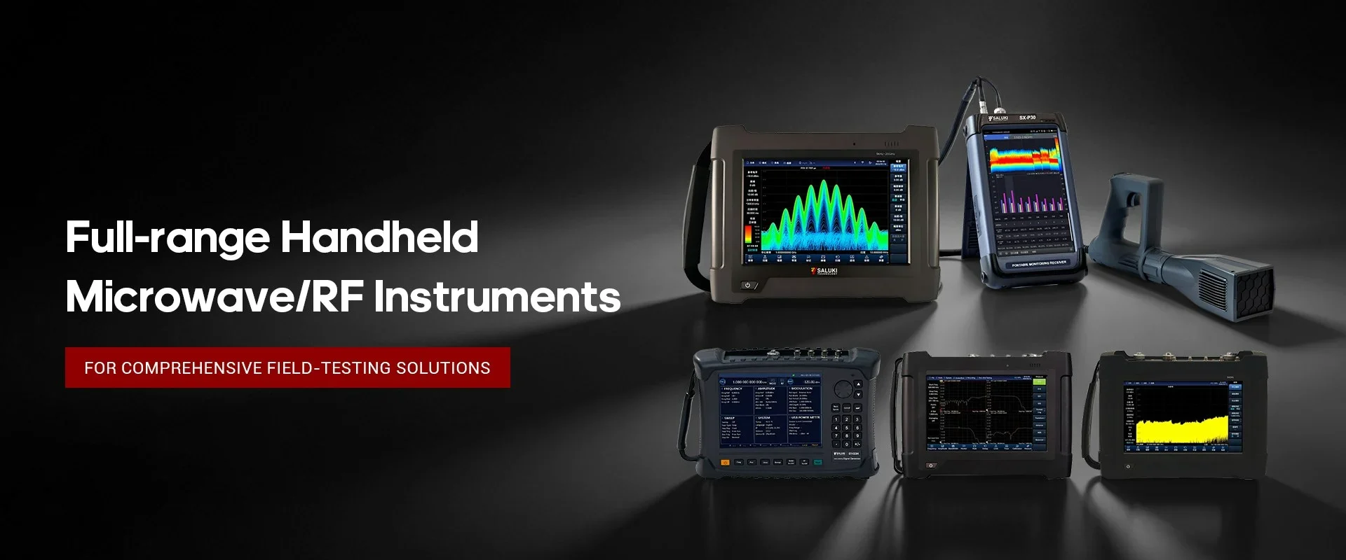
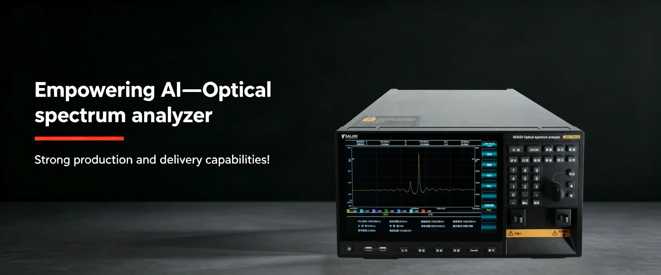
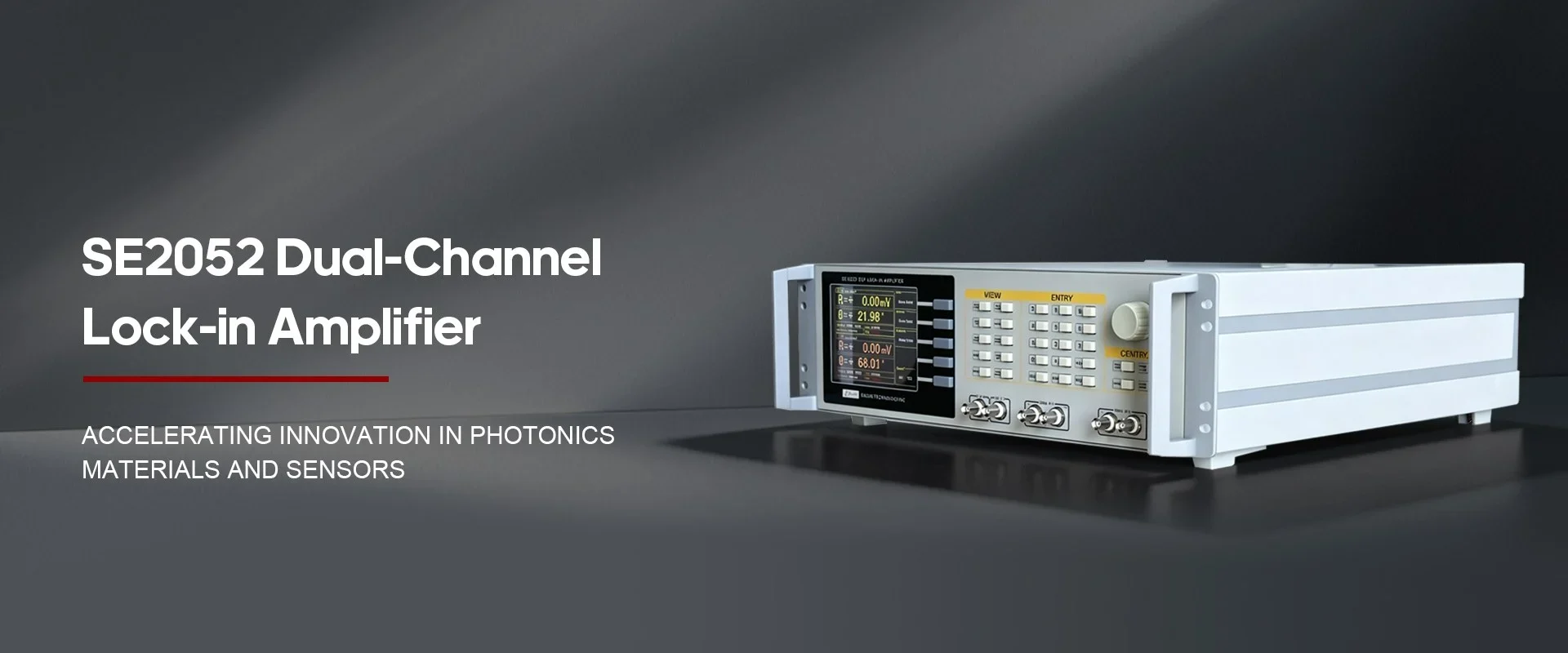
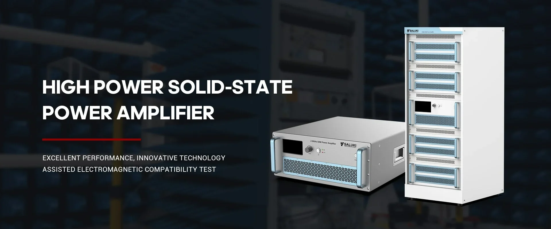

Best Selling Products
Contact us: sales@salukitec.com
As a professional RF, microwave, and millimeter-wave products manufacturer and supplier in China.
Whether you’re a reseller, distributor, solution provider, or startups, we have a solution to help you grow your business and bring new solutions to market. We believe it is a great opportunity for you to grow with us.

Company Profile
Overview
Saluki Technology Inc. is a high-tech company, supplier and manufacturer of High-end RF&MW Test Equipment, General Test Equipment, Lab Equipment and Optical Communication Equipment. Founded in 1997, the company was initially an agent of telecommunication equipment, and it once ranked second in the Chinese market. With an in-depth understanding of the market and user needs, meantime a deep accumulation of technology, the company began to develop its own brand of test equipment in 2008, and promoted it mainly for the Asian market. Beginning in 2015, the company moved its headquarters to Taiwan, and began to face more overseas markets and built the SALUKI brand.
At present, the company has exclusive agents in South Korea, Turkey, and stable partners in markets of countries like Canada, Germany, the United States, the United Kingdom, Finland, Poland, Indonesia, Israel, Vietnam, and South America.
We are committed to establishing a stable partnership with local agents to provide customers with the most professional, fast and long-term services.
Our Vision
Accurate, Fast and Reliable
-
20+
Work Experiences
-
100+
Sales Engineers
-
10+
Branch Openings
We can also provide the following brands
Lock-in Amplifier Applications and Working Principles in Typical Scenarios |
Lock-in amplifiers have a broad range of applications, including temperature detection, photoelectric detection, biosignal detection, and geological exploration. Below is a detailed introduction to two typical application scenarios.
1. Solar Cell Quantum Efficiency Measurement |
1.1 Two Types of Quantum Efficiency |
Solar cell quantum efficiency is divided into external quantum efficiency and internal quantum efficiency:
- External Quantum Efficiency (EQE): The ratio of the number of charge carriers generated in a solar cell to the number of incident photons of a given energy reaching the cell surface.
- Internal Quantum Efficiency (IQE): The ratio of the number of charge carriers generated in a solar cell to the number of photons of a given energy that are not reflected and not transmitted through the cell surface.
1.2 Test System and Working Principle |
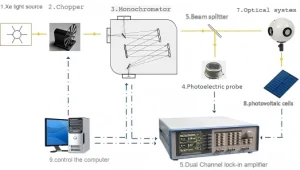
A solar cell quantum efficiency measurement system consists of a dual-channel lock-in amplifier, optical chopper, monochromator and other core devices. The probe light emitted from the monochromator is split into two beams: one beam is converted into photocurrent and fed into the lock-in amplifier as a reference; the other beam irradiates the solar cell, and the resulting photocurrent is measured by the second channel of the lock-in amplifier.
The ratio of the two channel measurements, combined with relevant formulas, is used to calculate the quantum efficiency of the solar cell.
2.Scanning Tunneling Spectroscopy Application |
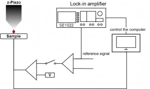
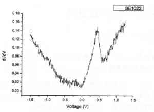
Scanning Tunneling Spectroscopy (STS) performs I-V or dI/dV-V measurements at a fixed position on the sample surface to obtain scanning tunneling spectra with characteristic peaks. At the voltage corresponding to the characteristic peak, with the average current kept constant, the tip scans across the X-Y plane to measure the variation of dI/dV with X and Y coordinates, producing a scanning tunneling spectroscopy image. The electronic and chemical properties of the sample surface can be characterized via I-V curves and dI/dV-V spectra.
Related products: |
Lock-In Amplifiers: Principle, Applications & Products | Saluki Technology
♦ Need technical support or a custom solution? Contact our application engineers: saluki@salukitec.com.
♦ To request a quotation, please contact sales@salukitec.com or click “Contact Us“ to leave a message.
