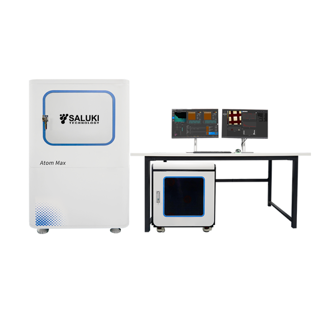
The microcantilever probe structure enables three-dimensional morphological characterization of solid materials such as conductors, semiconductors, and insulators, achieving wafer-level large sample morphology characterization. The motorized sample positioning stage, combined with optical imaging, achieves a positioning accuracy of 1 µm within a 200 x 200 mm area. The optical structure and scanning head are integrated into one unit, making operation convenient.
Wafer-Level Atomic Force Microscope-Max
Key Features
50pm ultra-high vertical resolution
Intelligent focusing, needle insertion, and parameter adjustment functions for simple operation
XYZ desktop scanner achieves distortion-free, realistic imaging
Integrated AI scientific research model with virtual expert support throughout the process
Self-developed AFM core "power source," FPGA high-speed controller system
Powerful functional configuration, featuring multi-functional measurement modes including nanoforce, magnetism, and electricity
Built-in powerful analysis software
| Technical Specifications | |
| Sample Size | 8-inch wafer, backward compatible |
| Scanning Range | Maximum 100 μm x 100 μm x 10 μm |
| Scanning Angle | 0-360° |
| Resolution | Z-axis closed-loop resolution 0.05 nm; X/Y closed-loop resolution 0.5 nm |
| Scanning Probe XY Direction Image Resolution | 32×32~4096×4096 |
| Operating Modes | Contact mode, tapping mode, phase imaging mode, lift-up mode, multi-directional scanning mode |
| Multifunctional Measurement | EFM, KPFM, PFM, MFM |
Main Machine
| Module No. | Item | Description |
| SAFM-MAX | Measurement mode | Sample Size: 8-inch wafer, backward compatible Scanning Range: Maximum 100 μm x 100 μm x 10 μm Scanning Angle: 0-360° Resolution: Z-axis closed-loop resolution 0.05 nm; X/Y closed-loop resolution 0.5 nm Scanning Probe XY Direction Image Resolution: 32×32~4096×4096 Operating Modes: Contact mode, tapping mode, phase imaging mode, lift-up mode, multi-directional scanning mode Multifunctional Measurement: Electrostatic Force Microscopy (EFM), Scanning Kelvin Microscopy (KPFM), Piezoelectric Microscopy (PFM), Magnetic Force Microscopy (MFM) |


